- 您现在的位置:买卖IC网 > Sheet目录1997 > ICS650R-14LFT (IDT, Integrated Device Technology Inc)IC NETWORKING SYSTEM CLK 20-SSOP
ICS650-14
NETWORKING SYSTEM CLOCK
CLOCK SYNTHESIZER
IDT / ICS NETWORKING SYSTEM CLOCK
4
ICS650-14
REV H 051310
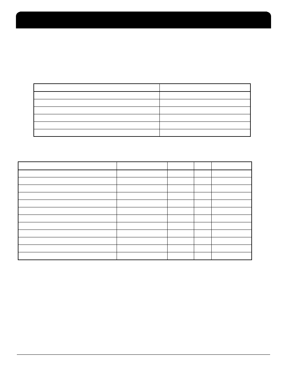
Absolute Maximum Ratings
Stresses above the ratings listed below can cause permanent damage to the ICS650-14. These ratings, which are
standard values for IDT commercially rated parts, are stress ratings only. Functional operation of the device at these
or any other conditions above those indicated in the operational sections of the specifications is not implied.
Exposure to absolute maximum rating conditions for extended periods can affect product reliability. Electrical
parameters are guaranteed only over the recommended operating temperature range.
DC Electrical Characteristics
Unless stated otherwise, VDD = 3.3 V ±10%, Ambient Temperature 0 to +70
° C
Item
Rating
Supply Voltage, VDD (referecned to GND)
7 V
Inputs and Outputs (referecned to GND)
-0.5 V to VDD+0.5 V
Ambient Operating Temperature
0 to +70
° C
Ambient Operating Temperature (industrial “I” version)
-40 to 85
° C
Soldering Temperature (max. of 20 seconds)
-65 to +150
° C
Storage Temperature
260
° C
Parameter
Symbol
Conditions
Min.
Typ.
Max.
Units
Operating Voltage
VDD
3.0
5.5
V
Input High Voltage (X1 pin only)
VIH
Clock input
VDD/2+1
V
Input Low Voltage (X1 pin only)
VIL
Clock input
VDD/2-1
V
Input High Voltage (SEL pins only)
VIH
VDD-0.5
V
Input Low Voltage (SEL pins only)
VIL
0.5
V
Input High Voltage (OE pin only)
VIH
2.0
V
Input Low Voltage (OE pin only)
VIL
0.8
V
Output High Voltage
VOH
IOH = -12 mA
2.4
V
Output High Voltage (CMOS level)
VOH
IOH = -8 mA
VDD-0.4
V
Output Low Voltage
VOL
IOL = 12 mA
0.4
V
Operating Supply Current
IDD
No load, VDD = 3.3 V
32
mA
Short Circuit Current
Each output
±50
mA
发布紧急采购,3分钟左右您将得到回复。
相关PDF资料
ICS650R-21ILF
IC CLK SOURCE SYSTEM PER 20-SSOP
ICS650R-22LF
IC CLK SOURCE PRV/STB 20-SSOP
ICS650R-27ILF
IC CLK SOURCE NETWORK 20-SSOP
ICS663MILFT
IC PLL BUILDING BLOCK 8-SOIC
ICS667M-01LF
IC CLK SYNTHESIZER HDTV 8-SOIC
ICS670M-01ILFT
IC BUFFER/MULTIPLIER ZD 16-SOIC
ICS670M-03ILFT
IC BUFFER/MULTIPLIER ZD 16-SOIC
ICS670M-04ILF
IC BUFFER/MULTIPLIER ZD 16-SOIC
相关代理商/技术参数
ICS650R-14T
功能描述:IC NETWORKING SYSTEM CLK 20-SSOP RoHS:否 类别:集成电路 (IC) >> 时钟/计时 - 时钟发生器,PLL,频率合成器 系列:- 产品变化通告:Product Discontinuation 04/May/2011 标准包装:96 系列:- 类型:时钟倍频器,零延迟缓冲器 PLL:带旁路 输入:LVTTL 输出:LVTTL 电路数:1 比率 - 输入:输出:1:8 差分 - 输入:输出:无/无 频率 - 最大:133.3MHz 除法器/乘法器:是/无 电源电压:3 V ~ 3.6 V 工作温度:0°C ~ 70°C 安装类型:表面贴装 封装/外壳:16-TSSOP(0.173",4.40mm 宽) 供应商设备封装:16-TSSOP 包装:管件 其它名称:23S08-5HPGG
ICS650R-21
功能描述:IC CLK SOURCE SYSTEM PER 20-SSOP RoHS:否 类别:集成电路 (IC) >> 时钟/计时 - 时钟发生器,PLL,频率合成器 系列:- 产品变化通告:Product Discontinuation 04/May/2011 标准包装:96 系列:- 类型:时钟倍频器,零延迟缓冲器 PLL:带旁路 输入:LVTTL 输出:LVTTL 电路数:1 比率 - 输入:输出:1:8 差分 - 输入:输出:无/无 频率 - 最大:133.3MHz 除法器/乘法器:是/无 电源电压:3 V ~ 3.6 V 工作温度:0°C ~ 70°C 安装类型:表面贴装 封装/外壳:16-TSSOP(0.173",4.40mm 宽) 供应商设备封装:16-TSSOP 包装:管件 其它名称:23S08-5HPGG
ICS650R-21I
功能描述:IC CLK SOURCE SYSTEM PER 20-SSOP RoHS:否 类别:集成电路 (IC) >> 时钟/计时 - 时钟发生器,PLL,频率合成器 系列:- 产品变化通告:Product Discontinuation 04/May/2011 标准包装:96 系列:- 类型:时钟倍频器,零延迟缓冲器 PLL:带旁路 输入:LVTTL 输出:LVTTL 电路数:1 比率 - 输入:输出:1:8 差分 - 输入:输出:无/无 频率 - 最大:133.3MHz 除法器/乘法器:是/无 电源电压:3 V ~ 3.6 V 工作温度:0°C ~ 70°C 安装类型:表面贴装 封装/外壳:16-TSSOP(0.173",4.40mm 宽) 供应商设备封装:16-TSSOP 包装:管件 其它名称:23S08-5HPGG
ICS650R-21ILF
功能描述:IC CLK SOURCE SYSTEM PER 20-SSOP RoHS:是 类别:集成电路 (IC) >> 时钟/计时 - 时钟发生器,PLL,频率合成器 系列:- 标准包装:1,000 系列:- 类型:时钟/频率合成器,扇出分配 PLL:- 输入:- 输出:- 电路数:- 比率 - 输入:输出:- 差分 - 输入:输出:- 频率 - 最大:- 除法器/乘法器:- 电源电压:- 工作温度:- 安装类型:表面贴装 封装/外壳:56-VFQFN 裸露焊盘 供应商设备封装:56-VFQFP-EP(8x8) 包装:带卷 (TR) 其它名称:844S012AKI-01LFT
ICS650R-21ILFT
功能描述:IC CLK SOURCE SYSTEM PER 20-SSOP RoHS:是 类别:集成电路 (IC) >> 时钟/计时 - 时钟发生器,PLL,频率合成器 系列:- 标准包装:2,000 系列:- 类型:PLL 时钟发生器 PLL:带旁路 输入:LVCMOS,LVPECL 输出:LVCMOS 电路数:1 比率 - 输入:输出:2:11 差分 - 输入:输出:是/无 频率 - 最大:240MHz 除法器/乘法器:是/无 电源电压:3.135 V ~ 3.465 V 工作温度:0°C ~ 70°C 安装类型:表面贴装 封装/外壳:32-LQFP 供应商设备封装:32-TQFP(7x7) 包装:带卷 (TR)
ICS650R-21IT
功能描述:IC CLK SOURCE SYSTEM PER 20-SSOP RoHS:否 类别:集成电路 (IC) >> 时钟/计时 - 时钟发生器,PLL,频率合成器 系列:- 产品变化通告:Product Discontinuation 04/May/2011 标准包装:96 系列:- 类型:时钟倍频器,零延迟缓冲器 PLL:带旁路 输入:LVTTL 输出:LVTTL 电路数:1 比率 - 输入:输出:1:8 差分 - 输入:输出:无/无 频率 - 最大:133.3MHz 除法器/乘法器:是/无 电源电压:3 V ~ 3.6 V 工作温度:0°C ~ 70°C 安装类型:表面贴装 封装/外壳:16-TSSOP(0.173",4.40mm 宽) 供应商设备封装:16-TSSOP 包装:管件 其它名称:23S08-5HPGG
ICS650R-21LF
功能描述:IC CLK SOURCE SYSTEM PER 20-SSOP RoHS:是 类别:集成电路 (IC) >> 时钟/计时 - 时钟发生器,PLL,频率合成器 系列:- 标准包装:2,000 系列:- 类型:PLL 频率合成器 PLL:是 输入:晶体 输出:时钟 电路数:1 比率 - 输入:输出:1:1 差分 - 输入:输出:无/无 频率 - 最大:1GHz 除法器/乘法器:是/无 电源电压:4.5 V ~ 5.5 V 工作温度:-20°C ~ 85°C 安装类型:表面贴装 封装/外壳:16-LSSOP(0.175",4.40mm 宽) 供应商设备封装:16-SSOP 包装:带卷 (TR) 其它名称:NJW1504V-TE1-NDNJW1504V-TE1TR
ICS650R-21LFT
功能描述:IC CLOCK SYNTHESIZER 20-SSOP RoHS:是 类别:集成电路 (IC) >> 时钟/计时 - 时钟发生器,PLL,频率合成器 系列:- 标准包装:2,000 系列:- 类型:PLL 时钟发生器 PLL:带旁路 输入:LVCMOS,LVPECL 输出:LVCMOS 电路数:1 比率 - 输入:输出:2:11 差分 - 输入:输出:是/无 频率 - 最大:240MHz 除法器/乘法器:是/无 电源电压:3.135 V ~ 3.465 V 工作温度:0°C ~ 70°C 安装类型:表面贴装 封装/外壳:32-LQFP 供应商设备封装:32-TQFP(7x7) 包装:带卷 (TR)